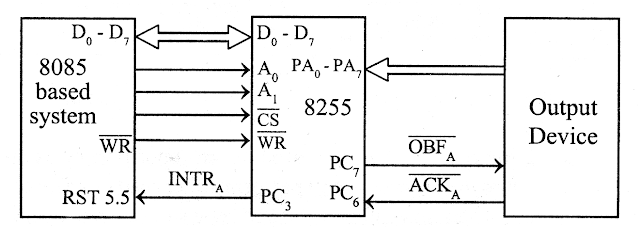
Interfacing Intel 8251A with 8085 Processor

The 825 1A can be either memory mapped or I/O mapped in the system.

•    8251A in I/O mapped in the system is shown in the figure.

•    Using a 3-to-8 decoder generates the chip select signals for I/O mapped devices.

•    The address lines A4, A5  and A6  are decoded to generate eight chip select signals (IOCS-0
to IOCS-7) and in this, the chip select signal IOCS-2 is used to select 8251A.

•    The address line A7  and the control signal IO / M(low) are used as enable for decoder.

•    The address line  A0  of 8085 is connected to  C/D(low) of 8251A to provide the internal addresses.

•    The data lines D0  – D7  are connected to D0  – D7  of the processor to achieve parallel data transfer.

•    The RESET and clock signals are supplied by the processor. Here the processor clock is directly  connected  to  8251A.  This  clock  controls  the  parallel  data  transfer  between  the processor and 8251A.

•    The output clock signal of 8085 is divided by suitable clock dividers like programmable timer 8254 and then used as clock for serial transmission and reception.

•    The TTL logic levels of the serial data lines  and the control signals necessary for serial transmission and reception are converted to RS232 logic levels using MAX232 and then terminated on a standard 9-pin D-.type connector.

•    In 8251A the transmission and reception baud rates can be different or same.


•    The device which requires serial communication with processor can be connected to this
9-pin D-type connector using 9-core cable.

•    The signals TxEMPTY, TxRDY and RxRDY can be used as interrupt signals to initiate interrupt driven data transfer scheme between processor and 8251 A.

•    I/O addresses of 8251A interfaced to 8085 is,


USART-INTEL 8251A MICROPROCESSOR

The  8251A  is  a  programmable  serial  communication  interface  chip  designed  for synchronous and asynchronous serial data communication.It supports the serial transmission of data.It is packed in a 28 pin DIP.
Pin Diagram of 8251A

Block Diagram:

The functional block diagram of 825 1A consists five sections. They are

•    Read/Write control logic
•    Transmitter
•    Receiver
•    Data bus buffer
•    Modem control.

  The functional block diagram is,


Functional block diagram of 8251A-USART


Read/Write control logic:

•    The Read/Write Control logic interfaces the 8251A with CPU, determines the functions of the 8251A according to the control word written into its control register.

•    It monitors the data flow.

•    This  section  has  three  registers  and  they  are  control  register,  status  register  and  data buffer.

•    The active low signals RD, WR, CS and C/D(Low) are used for read/write operations with these three registers.

•    When C/D(low) is high, the control register is selected for writing control word or reading status word.

•    When C/D(low) is low, the data buffer is selected for read/write operation.

•    When the reset is high, it forces 8251A into the idle mode.

•    The clock input is necessary for 8251A for communication with CPU and this clock does not control either the serial transmission or the reception rate.

Transmitter section:

•    The transmitter section accepts parallel data from CPU and converts them into serial data.

•    The  transmitter  section  is  double  buffered,  i.e.,  it  has  a  buffer  register  to  hold  an  8-bit parallel  data  and  another  register  called  output  register  to  convert  the  parallel  data  into
serial bits.

•    When output register is empty, the data is transferred from buffer to output register. Now the processor can again load another data in buffer register.

•    If buffer register is empty, then TxRDY is goes to high.

•    If output register is empty then TxEMPTY goes to high.

•    The  clock  signal,  TxC  (low)  controls  the  rate  at  which  the  bits  are  transmitted  by  the
USART.

•    The clock frequency can be 1,16 or 64 times the baud rate.

Receiver Section:


•    The receiver section accepts serial data and convert them into parallel data.

•    The receiver section is double buffered, i.e., it has an input register to receive serial data and convert to parallel, and a buffer register to hold the parallel data.

•    When the RxD line goes low, the control logic assumes it as a START bit, waits for half a
bit time and samples the line again.

•    If the line is still low, then the input register accepts the following bits, forms a character and loads it into the buffer register.

•    The CPU reads the parallel data from the buffer register.

•    When the input register loads a parallel data to buffer register, the RxRDY line goes high.

•    The clock signal RxC (low) controls the rate at which bits are received by the USART.

•    During asynchronous mode, the signal SYNDET/BRKDET will indicate the break in the data transmission.

•    During synchronous mode, the signal  SYNDET/BRKDET will indicate the reception of synchronous character.

MODEM Control:

•    The MODEM control unit allows to interface  a MODEM to 8251A and to establish data communication through MODEM over telephone lines.

•    This unit takes care of handshake signals for MODEM interface.

KEYBOARD AND DISPLAY INTERFACE USING INTEL 8279 MICROPROCESSOR

In a microprocessor b   system,   when   keyboard   and   7-segment   LED   display   is interfaced using ports or latches then the processor has to carry the following task.

• Keyboard scanning
• Key debouncing
• Key code generation
• Sending display code to LED
• Display refreshing


Interfacing 8279 with 8085 processor:

 •    A  typical  Hexa  keyboard  and  7-segment  LED  display  interfacing  circuit  using  8279  is shown.


•    The  circuit  can  be  used  in  8085  microprocessor  system  and  consist  of  16  numbers  of hexa-keys and 6 numbers of 7-segment LEDs.

•    The 7-segment LEDs can be used to display six digit alphanumeric character.

•    The 8279 can be either memory mapped or I/O mapped in the system. In the circuit shown
is the 8279 is I/O mapped.

•    The address line A0 of the system is used as A0 of 8279.

•    The clock signal for  8279 is obtained by dividing the output clock signal of  8085 by  a clock divider circuit.

•    The chip select signal is obtained from the I/O address decoder of the 8085 system. The chip select signals for I/O mapped devices are generated by using a 3-to-8 decoder.

•    The address lines A4, A5 and A6 are used as input to decoder.

•    The address line A7 and the control signal IO/M (low) are used as enable for decoder.

•    The chip select signal IOCS-3 is used to select 8279.

•    The I/O address of the internal devices of 8279 are shown in table.


•    The circuit has 6 numbers of 7-segment LEDs and so the 8279 has to be programmed in encoded  scan.  (Because  in  decoded  scan,  only  4  numbers  of  7-segment  LEDs  can  be interfaced):

•    In encoded scan the output of scan lines will be binary count. Therefore an external, 3-to-
8 decoder is used to decode the scan lines SL0, SL1  and SL2  of 8279 to produce eight scan lines S0 to S7.

•    The decoded scan lines S0 and S1  are common for keyboard and display.

•    The decoded scan lines S2  to S5  are used only for display and the decoded scan lines S6
and S7 are not used in the system.

•    Anode and Cathode drivers are provided to take care of the current requirement of LEDs.

•    The pnp transistors, BC 158 are used as driver transistors.

•    The anode drivers are called segment drivers and cathode drivers are called digit drivers.

•    The 8279 output the display code for one digit through its output lines (OUT A0  to OUT
A3 and OUT B0 to OUT B3) and send a scan code through, SL0- SL3.

•    The display code is inverted by segment drivers and sent to segment bus.

•    The  scan  code  is  decoded  by  the  decoder  and  turns  ON  the  corresponding digit  driver. Now  one  digit  of  the  display  character  is  displayed.  After  a  small  interval  (10  milli- second, typical), the display is turned OFF (i.e., display is blanked) and the above process
is repeated for next digit. Thus multiplexed display is performed by 8279.

•    The keyboard matrix is- formed using the return lines, RL0 to RL3 of 8279 as columns and decoded scan lines S0 and S1 as rows.

•    A hexa key is placed at the crossing point of each row and column. A key press will short the row and column. Normally the column and row line will be high.

•    During scanning the 8279 will output binary  count on SL0  to SL3, which is decoded  by decoder to make a row as zero. When a row is zero the 8279 reads the columns. If there is
a key press then the corresponding column will be zero.

•    If 8279 detects a key press then it wait for debounce time and again read the columns to generate key code.

•    In encoded scan keyboard mode, the 8279 stores an 8-bit code for each valid key press. The keycode consist of the binary value of the column and row in which the key is found and the status of shift and control key.

•    After a scan time, the next row is made zero and the above process is repeated and so on. Thus 8279 continuously scan the keyboard.


Interfacing 8279 with 8086 processor:

• A  typical  Hexa  keyboard  and  7-segment  LED  display  interfacing  circuit  using  8279  f
8086 based system is shown.


•        The system consists of 16 numbers of hexa-keys and numbers of 7-segment LEDs. The 7- segment LEDs can be used to display eight-digit alphanumeric character.

•    The 8279 can be either memory mapped or I/O mapped in the system. In the circuit shown
is I/O mapped.

•    The address line A1 of the system is used as A0 of 8279.

•    The clock signal for 8279 is obtained by dividing the PCLK (peripheral clock) of 8284 by
a clock divider circuit.

•    The chip select signals, for I/O mapped devices are generated by using a 3-to-8 decoder.

•    The address lines A5, A6 and A7 are used as input to decoder.

•    The address line A0  and the control signal M  /IO (low) are used as enable for decoder. The chip select signal IOCS-3 is used to select 8279.

•    The I/O address of the internal devices of 8279 is shown in table.


•    The circuit has 6 numbers of 7-segment LEDs and so the 8279 has to be programmed in encoded  scan.  (Because  in  decoded  scan,  only  4  numbers  of  7-segment  LEDs  can  be interfaced):

•    In encoded scan the output of scan lines will be binary count. Therefore an external, 3-to-
8 decoder is used to decode the scan lines SL0, SL1  and SL2  of 8279 to produce eight scan lines S0 to S7.

•    The decoded scan lines S0 and S1  are common for keyboard and display.

•    The decoded scan lines S2  to S5  are used only for display and the decoded scan lines S6
and S7 are not used in the system.

•    Anode and Cathode drivers are provided to take care of the current requirement of LEDs.

•    The pnp transistors, BC 158 are used as driver transistors.

•    The anode drivers are called segment drivers and cathode drivers are called digit drivers.

•    The 8279 output the display code for one digit through its output lines (OUT A0  to OUT
A3 and OUT B0 to OUT B3) and send a scan code through, SL0- SL3.

•    The display code is inverted by segment drivers and sent to segment bus.

•    The  scan  code  is  decoded  by  the  decoder  and  turns  ON  the  corresponding digit  driver. Now  one  digit  of  the  display  character  is  displayed.  After  a  small  interval  (10  milli-
second, typical), the display is turned OFF (i.e., display is blanked) and the above process
is repeated for next digit. Thus multiplexed display is performed by 8279.

•    The keyboard matrix is- formed using the return lines, RL0 to RL3 of 8279 as columns and decoded scan lines S0 and S1 as rows.

•    A hexa key is placed at the crossing point of each row and column. A key press will short the row and column. Normally the column and row line will be high.

•    During scanning the 8279 will output binary  count on SL0  to SL3, which is decoded  by decoder to make a row as zero. When a row is zero the 8279 reads the columns. If there is
a key press then the corresponding column will be zero.

•    If 8279 detects a key press then it wait for debounce time and again read the columns to generate key code.

•    In encoded scan keyboard mode, the 8279 stores an 8-bit code for each valid key press. The keycode consist of the binary value of the column and row in which the key is found
and the status of shift and control key.

•    After a scan time, the next row is made zero and the above process is repeated and so on. Thus 8279 continuously scan the keyboard.

INTEL 8279 MICROPROCESSOR - KEYBOARD/DISPLAY CONTROLLER

The INTEL 8279 is specially developed for interfacing keyboard and display devices
to 8085/8086/8088 microprocessor based system. The important features of 8279 are,

• Simultaneous keyboard and display operations.
• Scanned keyboard mode.
• Scanned sensor mode.
• 8-character keyboard FIFO.
• 1 6-character display.
• Right or left entry 1 6-byte display RAM.
• Programmable scan timing.

Block diagram of 8279:

•    The functional block diagram of 8279 is shown.


•    The four major sections of 8279 are keyboard, scan, display and CPU interface.

Keyboard section:

•    The keyboard section consists of eight return lines RL0 – RL7 that can be used to form the columns of a keyboard matrix.

•    It   has   two   additional   input   :   shift   and   control/strobe.   The   keys   are   automatically debounced.

•    The two operating modes of keyboard section are 2-key lockout and N-key rollover.

•    In the 2-key lockout mode, if two keys are pressed simultaneously, only the first key is recognized.

•    In the N-key rollover mode simultaneous keys are recognized and their codes are stored in
FIFO.

•    The keyboard section also have an 8 x 8 FIFO (First In First Out) RAM.

•    The FIFO can store eight key codes in the scan keyboard mode. The status of the shift key and control key are also stored along with key code. The 8279 generate an interrupt signal when there is an entry in FIFO. The format of key code entry in FIFO for scan keyboard mode is,


•    In sensor  matrix mode the condition (i.e., open/close status) of 64  switches is stored in FIFO RAM. If the condition of any of the switches changes then the 8279 asserts IRQ as high to interrupt the processor.

Display section:

•    The display section has eight output lines divided into two groups A0-A3 and B0-B3.

•    The output lines can be used either as a single group of eight lines or as two  groups of four lines, in conjunction with the scan lines for a multiplexed display.

•    The output lines are connected to the anodes through driver transistor in case of common cathode 7-segment LEDs.

•    The cathodes are connected to scan lines through driver transistors.

•    The display can be blanked by BD (low) line.

•    The display section consists of 16 x 8 display RAM. The CPU can read from or write into any location of the display RAM.

Scan section:


•    The scan section has a scan counter and four scan lines, SL0 to SL3.

•    In decoded scan mode, the output of scan lines will be similar to a 2-to-4 decoder.

•    In encoded scan mode, the output of scan lines will be binary count, and so an external decoder should be used to convert the binary count to decoded output.

•    The scan lines are common for keyboard and display.

•    The scan lines are used to form the rows of a matrix keyboard and also connected to digit drivers of a multiplexed display, to turn ON/OFF.

CPU interface section:

•    The CPU interface section takes care of data transfer between 8279 and the processor.

•    This section has eight bidirectional data lines DB0  to DB7  for data transfer between 8279
and CPU.

•    It  requires  two  internal  address  A  =0  for  selecting  data  buffer  and  A  =  1  for  selecting control register of8279.

•    The control signals WR (low), RD (low), CS (low) and A0 are used for read/write to 8279.

•    It has an interrupt request line IRQ, for interrupt driven data transfer with processor.

•    The  8279  require  an  internal  clock  frequency  of  100  kHz.  This  can  be  obtained  by dividing the input clock by an internal prescaler.

•    The RESET signal sets the 8279 in 16-character display with two -key lockout keyboard modes.

Programming the 8279:

•    The  8279  can  be  programmed  to  perform  various  functions  through  eight  command words.

INTEL 8255 Programmable Peripheral Interface (PART-2)

Internal block diagram of 8255

The ports are grouped as Group A and Group B. The group A has port A, port C upper and its control circuit. The group B has port B, port C lower and its control circuit. The Read/Write control logic requires six control signals. These signals are given below.


RD (Read) :   This control signal enables the read operation.
                     When this signal is LOW, the microprocessor reads data from a selected I/O port of the 
                      8255A.

WR (Write):  This control signal enables the write operation.
                       When this signal goes LOW, the microprocessor writes into a selected I/O port
                       or the control register.

RESET:         This is an active HIGH signal.
                       It clears the control register and set all ports in the input mode.

CS, A0  and A1 : These are device select signals.
                             The CS is connected to the decoder in the system.
                             A0 and A1 are generally connected to A0 and A1 of the processor.

(Alternatively, A0 and A1 can be connected to any two-address lines of the processor).
8255 can be either Memory mapped or I/O mapped in the system.

A0 and A1 address lines can be made to select any one of the following four internal devices as shown on right side.


Programming 8255:
The 8255 has two control words, one for specifying 1/O functions and another for bit set/reset mode of port C. Both the control words are written in the same control register.

The control register differentiate them by the value of bit D7 .The bit set/reset control word does not affect the functions of ports A and B.

Bit D7 of the control register specifies either the 1/0 function or the bit set / reset function.
If bit D7 = 1, then the bits D6 – D0 determine 1/0 functions in various modes.
If bit D7 = 0, then the bits D6 – D0 determine the pin of port C to be set or reset.


The 8255 ports are programmed (or initialized) by writing a control word in the control register.

For setting 1/0 functions
and mode of operation the 1/0 mode control word is send to control register. The format of the 1/0 mode set control word is shown below.

For setting/resetting (BSR mode) a pin of port C, the bit set/ reset control word is sent to control register. The format of bit set/reset control word is shown below.


The data transfer between the processor and the port can be either interrupt driven or through status check.

In the interrupt driven data transfer scheme, when the port is ready, it interrupts the processor for a read or write operation.

In status check technique, the processor polls the status of the port and checks whether the port is ready for data transfer or not. The status of the ports A and B can be known by reading the port C. When the port is ready for data transfer, the processors executes a read or write cycle.

INTEL 8255 Programmable Peripheral Interface (PART-1)

Intel 8255 is a programmable peripheral interface chip designed for parallel communication between microprocessor and I/O devices, which have a speed mismatch between each other.


Features of 8255:

•It has three 8-bit ports
•It can be operated in three different modes in I/O mode and in BSR mode

IC 8255 has three ports A, Band C. The ports A and B are 8 bit parallel ports. Port A can be programmed to work in any one of the three modes as input or output port. The three operating modes are

Mode-0  - Simple I/O port
Mode-l   - Handshake I/O port
Mode-2  - Bidirectional I/O port.


The port B can be programmed to work either in mode-0 or mode-1. The port C pins (8-pins) have different assignments depending on the mode of port A and B. If port A and B are programmed in mode-0, then the port C can perform anyone of the following function.

1. As 8 bit parallel port in mode-0 for input or output.
2. As two numbers of 4 bit parallel port in mode-O for input or output.
3. The individual pins of port C can be set or reset for various control applications.

The various functions (assignments) of port C during the different operating modes of port A and B are listed in Table below.


If ports A and Bare programmed in mode-l or mode-2, then some of the pins of port C are used for handshake signals and the remaining pins can be used as input/output lines or individually set/reset for control applications.


I/0 Modes of 8255

Mode-0: In this mode, all the three ports can be programmed either as input or output port. In mode-O, the outputs are latched and the inputs are not latched. The ports do not have handshake or Interrupt capability. The ports in mode-o can be used to interface DIP switches, Hexa-keypad, LED's and 7-segment LED's to the processor.

Mode-l: In this mode, only ports A & B can be programmed either as input or output port. In mode-1, handshake signals are exchanged between the processor and peripherals prior to data transfer. The port C pins are used for  handshake signals. Input and output data are latched. Interrupt driven data transfer scheme is possible.

8255 Handshake Input port (Mode 1)


8255 Handshake Output port (Mode 1)\


Mode-2: In this mode, the port will be a bi-directional port (i.e., the processor can perform both read and write operations with an I/O device connected to a port in mode-2).
Only port-A can be programmed to work in mode-2. Five pins of port C are used for handshake signals. This mode is used primarily in applications such as data transfer between two computers or floppy disk controller interface.


Pins & Signals of 8255

The pin description of 8255 is shown in figure below. It has 40 pins and requires a single +5V supply.


INTEL 8085 Processor - Question & Answers (part-2)

In  a microprocessor system using  8085,  the  memory  requirement  is 8kb  EPROM  and 8kb  RAM.  For  interfacing  I/O  devices,  three  numbers  of  8255  are  required.  Select suitable memories and explain how they are interfaced to the system. Interface the 8255 by memory mapping.?

    The IC 2764 is selected for EPROM memory and the IC 6264 is selected for RAM memory.
    Both the memory lC have time compatibility with 8085 processor.
    The  8kb  EPROM,  2764  require  13  address  tines.  The  8kb  RAM,  6264  require  13  address lines.
    The address lines A0 to A12  are connected to both EPROM and RAM memory ICs.
    The 8255 require four internal addresses.

    Let us connect A1  of 8085 to A0  of 8255 and A2  of 8085 to A1  of 8255.
    The 8255 is memory mapped in the system.
    For  the  memories  and  8255’ s we  require  5  chip-select  signals.  Hence  we  can  use  a  3-to-8 decoder  74LS138  for  generating  eight  chip-select  signals  by  decoding  the  unused  address lines A13, A14  and A15.
    The decoder enable pins are permanently tied to appropriate levels. In the eight chips select
signals five are used for selecting memory ICs and 8255, and the remaining three can be used for future expansion.
    The EPROM is mapped at the starting of memory space. The RAM is mapped at the end of memory space. The EPROM is  mapped  from 0000H to IFFFH. The RAM is  mapped from E000H to FFFFH.
    The  four  internal devices of 8255 are control register, port-A,  port-B and  port-C.  A 16-bit address is allotted to each internal device of 8255.

Memory and I/O Port Interfacing with 8085


The 16 bit address for the memory and 8255 devices are,


A  system  requires  16kb  EPROM  and  16kb  RAM.  Also  the  system  has  2  numbers  of 8255, one number of 8279, one number of 8251 and one number of 8254. (8255 - Programmable peripheral  interface;  8279-Keyboard/display  controller,  8251  –  USART  and  8254  -  Timer). Draw the Interface diagram. Allocate addresses to all the devices. The peripheral IC should be I/O mapped.

• The  I/O  devices  in  the  system  should  be  mapped  by  standard  I/O  mapping.  Hence  separate decoders can be used to generate chip select signals for memory IC and peripheral IC’ s.
• For 16kb EPROM, we can provide 2 numbers of 2764(8k x 8) EPROM.

• For 16kb RAM we can provide 2 numbers of 6264 (8k x 8) RAM.

• The  8kb  memories  require  13  address  lines.  Hence  the  address  lines  A0   –  A12   are  used  for selecting the memory locations.
• The unused address lines A13, A14  and A15  are used as input to decoder 74LS138 (3-to-8-deeoder)

of memory IC.  The  logic  low  enables of this decoder are tied to  IO/ M(low) of 8085,  so that this decoder  is  enabled  for  memory read/write  operation.  The  other  enable  pins  of decoder  are tied  to appropriate logic levels permanently. The 4-outputs of the decoder are used to select memory lCs and
the remaining 4 are kept for future expansion.

• The EPROM is mapped in the beginning of memory space from 0000H to 3FFF.

•  The RAM is mapped at the end of memory space from C000 to FFFFH.

• There are five peripheral IC’ s to be interfaced to the system. The chip-select signals for these IC’ s

are given through another 3-to-8 decoder 74LS138 (I/O decoder). The input to this decoder is A11, A12  and A13
• The address lines A13, A14  and A15  are logically ORed and applied to low enable of I/O decoder.

• The logic high enable of I/O decoder is tied to IO / M(low) signal of 8085, so that this decoder is enabled for I/O read/write operation.

Memory and I/O Port Interfacing with 8085


INTEL 8085 Processor - Question & Answers (part-1)

Consider a system in which the full memory space 64kb is utilized for EPROM memory. Interface the EPROM with 8085 processor.
• The memory capacity is 64 Kbytes. i.e
          2 n = 64 x 1000 bytes where n = address lines. So, n = 16.

• In this  system the entire 16  address  lines of the processor are connected to  address input pins of memory IC in order to address the internal locations of memory.

• The  chip  select  (CS)  pin  of  EPROM  is  permanently  tied  to  logic  low  (i.e.,  tied  to ground).

• Since the processor  is connected to EPROM, the active  low  RD pin  is connected to active low output enable pin of EPROM.

• The range of address for EPROM is 0000H to FFFFH.


Interfacing 64Kb EPROM with 8085

Consider a system in which the available 64kb memory space is equally divided between
EPROM and RAM. Interface the EPROM and RAM with 8085 processor.


•    Implement 32kb memory capacity of EPROM using single IC 27256.

•    32kb RAM capacity is implemented using single IC 62256.

•    The 32kb memory requires 15 address lines and so the address lines A0  – A14  of the processor are connected to 15 address pins of both EPROM and RAM.

•    The unused address line A15  is used as to chip select. If A15  is 1, it select RAM and If
A15  is 0, it select EPROM.

•    Inverter is used for selecting the memory.

•    The memory used is both Ram and EPROM, so the low RD and WR pins of processor are connected to low WE and OE pins of memory respectively.

•    The  address  range  of  EPROM  will  be  0000H  to  7FFFH  and  that  of  RAM  will  be
7FFFH to FFFFH.


Interfacing 32Kb EPROM and 32Kb RAM with 8085


Consider a system in which 32kb memory space is implemented using four numbers of
8kb memory. Interface the EPROM and RAM with 8085 processor.


•    The total memory capacity is 32Kb. So, let two number of 8kb n memory be EPROM and the remaining two numbers be RAM.

•    Each 8kb memory requires 13 address lines and so the address lines A0- A12  of the processor are connected to 13 address pins of all the memory.

•    The address lines and A13  – A14  can be decoded using a 2-to-4 decoder to generate four chip select signals.

•    These  four chip  select  signals can  be used to  select  one of the  four  memory IC at  any one time.

•    The address line A15  is used as enable for decoder.

•    The simplified schematic memory organization is shown

Interfacing 16Kb EPROM and 16Kb RAM with 8085


•    The address allotted to each memory IC is shown in following table.


There are two types for interfacing I/O devices:

1.   Memory mapped I/O device.
2.   Standard I/O mapped I/O device or isolated I/O mapping.


DECODER IN 8085 PROCESSOR

It is used to select the memory chip of processor during the execution of a program.

No of IC used for decoder is,
  •   2-4 decoder (74LS139)
  •   3-8 decoder (74LS138)


TYPICAL EPROM AND STATIC RAM

A typical semiconductor memory IC will have n address pins, m data pins (or output pins).

•Having two power supply pins (one for connecting required supply voltage (V and the other for connecting ground).

•The control signals needed for static RAM are chip select (chip enable), read control (output enable) and write control (write enable).

•The  control signals  needed  for  read  operation  in  EPROM are  chip  select  (chip  enable)  and read control (output enable).


STRING INSTRUCTIONS IN 8086 PROCESSORS

• REP / REPE / REPZ / REPNE / REPNZ
• MOVS / MOVSB / MOVSW
• CMPS / CMPSB / CMPSW
• SCAS / SCASB / SCASW
• LODS / LODSB / LODSW
• STOS / STOSB / STOSW

ADDRESSING MODES:

1. Addressing modes for accessing immediate and register data.
2. Addressing modes for accessing data in memory.
3. Addressing modes for accessing I/O ports.
4. Relative Addressing mode.
5. Implied Addressing mode.

(1). Addressing modes for accessing immediate and register data:

(i) Register addressing mode: The registers, which is having the data to be operated is specified in the instruction.


• The IP content is,  [IP]new = [IP]old + 000AH.
• The effective address is, [EA] = [IP]new + 000AH.
• The base address is, BA = [CS] x 1610
• The memory address is, MA = [EA] + [BA].
• Program control jump into the new MA.

(5) Implied Addressing:

• The instruction itself is having the data to be operated.
• Eg. : CLC – It clears the carry flag.

8086 Instruction Set Part (4-10)

 4. SHIFT INSTRUCTIONS

SAL / SHL:

•The mnemonics is SAL / SHL destination, count.


Bit Manipulation Instruction Set (Logical Instructions) In 8086 Processors

NOT:  The NOT instruction inverts each bit of a byte or a word. The destination can be register or a memory location.
        Eg. :                    ; AL = 0110 1100
        NOT AL            ; AL = 1001 0011

                                   ; CX = 10101111 0010 0010
        NOT CX            ; CX = 0101 0000 11011001

AND: This instruction logically ANDs each bit of the source byte or word with the corresponding bit in the destination and stores result in the destination.

                 Eg. :               ; AL = 1001 0011 = 93H
                                       ; BL = 0111 0101 = 75H
    AND BL, AL              ; AND Byte in AL with byte in BL
                                       ; BL = 0001 0001 = 11H

OR : This instruction logically ORs each bit of the source byte or word with the corresponding bit in the destination and stores result in the destination.

                Eg. :           ; AL =1001 0011 = 93H
                                  ; BL =0111 0101 = 75H
    OR BL, AL            ; OR byte in AL with byte in BL
                                  ; BL =1111 0111 = F7H

XOR : This instruction logically XORs each bit of the source byte or word with the corresponding bit in the destination and stores result in the destination.

TEST: This instruction logically ANDs each bit of the source byte or word with the corresponding bit in the destination and updates the flags but not stores results in anywhere.

                 Eg. :            ; AL = 1001 0011 = 93H
                                    ; BL = 0111 0101 = 75H
    AND BL, AL           ; AND Byte in AL with byte in BL
                                    ; Result = 0001 0001 = 11H (not stored)
                                    ; Z  = 0, P = 1 (flag affected))
    AND BX, AX          ;  AND word in AX with word in BX
                                    ; updates the flag and result is not stored.

Arithmetic Instruction Set In 8086 Processors

(a) Addition


Instructions:
ADD  – It add the destination and source contents.


Data Transfer Instruction Set In 8086 Processors

The instructions that transfer data between registers, memory locations or segment registers.
It is again classified into four types. They are,

1.General purpose byte or word transfer instructions
2.Special address transfer instructions
3.Flag transfer instructions
4.Simple input and output Port transfer instructions

1.General purpose byte or word transfer instructions
MOV: It copies the content of source to the destination.
       Eg. :  MOV BX, 5978H    ; Load the immediate number 5978H to BX.
                MOV CL, [453AH] ; Copies the content of memory location which is at a distant of  453AH   from the data segment into CL register.
               MOV DS, CX          ; Copies the word from CX to data segment.
PUSH

• It decrements the stack pointer by 2.
• It stores the 16 bit data from the source to the address in the stack pointer.
Eg. :      SP = 80983H
     CX = 49A3H
        PUSH CX
                 SP = 80981H
                 [CX]----> SP

POP

•It stores the 16 bit data from the destination to the stack pointer.
•It increments the stack pointer by 2.

Eg. :      SP = 80983H
            CX = 49A3H
        POP CX
                  [CX]
                  SP = 80985H
XCHG: It exchanges the contents of source with the destination.
          Eg. : XCHG BX, CX   ;  Exchange word in CX with word in BX.
                 XCHG BL, CL     ;  Exchange byte in CL with byte in BL.

XLAT :

•IT replaces byte in AL register.
•BX is having the offset value of memory location.
•It copies byte from address pointed by [BX + AL ] into AL register.

2. Special address transfer instructions:

LEA:

   •Load effective address.
   •The mnemonics is LEA register, source.
   •Source is having the offset of the memory location and this instruction load      this address into 16 bit register.

LDS:

•The mnemonics is LDS register, memory address of first word.
•It copies a word from two memory locations into the register.
•It then copies a word from next two memory locations into the DS register.

Eg. : LDS CX, [391AH]

 LES:

•    The mnemonics is LES register, memory address of first word.
•    It copies a word from two memory locations into the register.
•    It then copies a word from next two memory locations into the ES register.

Eg. : LES CX, [391AH]

3. Flag Transfer Instructions:

LAHF  : This instruction copies the contents of lower byte of 8086 flag register to AH register.

SAHF  : The contents of the AH register are copied into the lower byte of the 8086 flag register.

PUSHF: This instruction decrements the stack pointer by 2 and copies the word in the flag register to   the memory locations pointed by the stack pointer.

POPF  : This instruction copies a word  the two memory locations at the top of the stack  to the flag  register and increments the stack pointer by 2.

4. Simple Input and Output Port Transfer Instructions:

IN  :

•This instruction will copy data from a port to the accumulator.
•If an 8 bit port is read the data will go to AL and if an 16 bit port is read the data will go to AX.

OUT :
The OUT instruction copies a byte from AL or a word from AX to the specified port.

ASSEMBLY LANGUAGE PROGRAMME OF 80X86 PROCESSORS

The general format of an assembler instruction is,
Label: Mnemonics Operand, Operand; comment.

 8086 instruction set is classified as follows.


4.String instruction.

5.Program execution transfer instruction.

6.Processor control instruction.

MAXIMUM MODE CONFIGURATION OF 8086 SYSTEM

• If the MN/MX (low) pin is low i.e. zero, then the 8086 can operate in maximum mode.

• In this mode, the Bus controller (8288) chip used to generate control signals I/O W, I/O R, RD., WR (Active low), etc., by receiving the active low status signals (S2, S1 & S0) from the microprocessor.

MRDC (low) : Memory read command – It instructs the memory to put the contents of the addressed location to the data bus.

MWTC (low) : Memory write command – It instructs the memory to accept the data on the data bus and load that data into the address memory location.

IORC (low) :  I/O read command – It instructs an I/O device to put the data contained in the addressed port on the data bus.

IOWC (low) : I/O write command – It instructs an I/O device to accept the data on the data bus and load the data into the addressed port.

AIOWC (low) / AMWC (low) : Advance IO write command / Advance memory write command – These are similar to IOWC and MWTC except that they are activated one clock pulse earlier. This gives slow interfaces an extra clock cycle to prepare to input the data.

• This system also consists of latches, tristate buffer, memory input-output device, etc.

• The DEN, DT/R, ALE, etc is derived by the bus controller from the information available on the active low status signals (S2, S1 & S0).

• In this mode, Request/Grant pin (RQ/GT) is checked at each rising pulse of clock I/P when the request is detected and if Hold request are satisfied, the processor issues a grant pulse over RQ/GT pin immediately during T4 or next T1 state to accept the control of the bus. Therefore, the requesting controller uses the bus till it requires.

• When it is ready to relinquish the bus, it sends a release pulse to the processor using the RQ/GT pin.

The figure shows maximum mode 8086 systems.


Maximum mode of 8086


MINIMUM MODE CONFIGURATION OF 8086 SYSTEM

• When MN/MX (low) pin is in logic 1, the 8086 microprocessor operates in minimum mode system.

• In this mode, the microprocessor chip itself gives out all the control signals.

• This is a single processor mode.

• The remaining components in the system are latches, trans receivers, clock generator, memory or I/O devices.

• This system has three address latches and two octal data buffers for the complete 20-bit address and 16 bit data Separation.

• The latches are used for separating the valid address from the multiplexed address/data signals and the controlled by the ALE signal generated by 8086.

• Transceivers are the bi-directional buffers. They are required to separate the valid data from the time multiplexed address/data signal. This is controlled by two signals, DEN & DT/R (low).

• DT/R (low) indicates that the direction of data, iei.e. from or to the indicator.

• DEN signal indicates the valid data is available on the data bus.

• This system contains memory for the monitor and users program storage. It also contains I/O devices to communicate with the processor.

• The clock generator in the system is used to generate the clock and to synchronize some external signals with the system clock.

• The minimum mode system organization is,


Minimum mode of 8086

8086 PIN CONFIGURATION

• The 16-bit 8086 microprocessor has 40 pins.
• It is available in 5 MH, 8MHz and 10 MHz.
• It can operate in two modes, i.e. single processor (minimum mode) or multiprocessor moth (maximum mode) configuration.
• The signals are categorized in three groups as follows

(i) Common signal, which are used in minimum as well as maximum mode
(ii) Signal for minimum mode
(iii) Signals for maximum mode.

• The pin diagram for 8086 processor is shown in fig.


• The signals common for both maximum & minimum modes are:


Pin From 24 to 31 in Minimum Mode:

         INTA (Interrupt Acknowledge) Output:  This indicates recognition of an interrupt request.


HOLD input, HLDA output:


• A HIGH on HOLD pin indicates that another master (DMA) is requesting to take over the system bus.
• On receiving HOLD signal processor outputs HLDA signal HIGH as an acknowledgment.
• At the same time, processor tristates the system bus.
• A low on HOLD gives the system bus control back to the processor. Processor then outputs low signal on HLDA.

Pin Definitions (24 to 31) In Maximum Mode:


Labels

PROJECTS 8086 PIN CONFIGURATION 80X86 PROCESSORS TRANSDUCERS 8086 – ARCHITECTURE Hall-Effect Transducers INTEL 8085 OPTICAL MATERIALS BIPOLAR TRANSISTORS INTEL 8255 Optoelectronic Devices Thermistors thevenin's theorem MAXIMUM MODE CONFIGURATION OF 8086 SYSTEM ASSEMBLY LANGUAGE PROGRAMME OF 80X86 PROCESSORS POWER PLANT ENGINEERING PRIME MOVERS 8279 with 8085 MINIMUM MODE CONFIGURATION OF 8086 SYSTEM MISCELLANEOUS DEVICES MODERN ENGINEERING MATERIALS 8085 Processor- Q and A-1 BASIC CONCEPTS OF FLUID MECHANICS OSCILLATORS 8085 Processor- Q and A-2 Features of 8086 PUMPS AND TURBINES 8031/8051 MICROCONTROLLER Chemfet Transducers DIODES FIRST LAW OF THERMODYNAMICS METHOD OF STATEMENTS 8279 with 8086 HIGH VOLTAGE ENGINEERING OVERVOLATGES AND INSULATION COORDINATION Thermocouples 8251A to 8086 ARCHITECTURE OF 8031/8051 Angle-Beam Transducers DATA TRANSFER INSTRUCTIONS IN 8051/8031 INSTRUCTION SET FOR 8051/8031 INTEL 8279 KEYBOARD AND DISPLAY INTERFACES USING 8279 LOGICAL INSTRUCTIONS FOR 8051/8031 Photonic Transducers TECHNOLOGICAL TIPS THREE POINT STARTER 8257 with 8085 ARITHMETIC INSTRUCTIONS IN 8051/8031 LIGHTNING PHENOMENA Photoelectric Detectors Physical Strain Gage Transducers 8259 PROCESSOR APPLICATIONS OF HALL EFFECT BRANCHING INSTRUCTIONS FOR 8051/8031 CPU OF 8031/8051 Capacitive Transducers DECODER Electromagnetic Transducer Hall voltage INTEL 8051 MICROCONTROLLER INTEL 8251A Insulation Resistance Test PINS AND SIGNALS OF 8031/8051 Physical Transducers Resistive Transducer STARTERS Thermocouple Vacuum Gages USART-INTEL 8251A APPLICATIONs OF 8085 MICROPROCESSOR CAPACITANCE Data Transfer Instructions In 8086 Processors EARTH FAULT RELAY ELECTRIC MOTORS ELECTRICAL AND ELECTRONIC INSTRUMENTS ELECTRICAL BREAKDOWN IN GASES FIELD EFFECT TRANSISTOR (FET) INTEL 8257 IONIZATION AND DECAY PROCESSES Inductive Transducers Microprocessor and Microcontroller OVER CURRENT RELAY OVER CURRENT RELAY TESTING METHODS PhotoConductive Detectors PhotoVoltaic Detectors Registers Of 8051/8031 Microcontroller Testing Methods ADC INTERFACE AMPLIFIERS APPLICATIONS OF 8259 EARTH ELECTRODE RESISTANCE MEASUREMENT TESTING METHODS EARTH FAULT RELAY TESTING METHODS Electricity Ferrodynamic Wattmeter Fiber-Optic Transducers IC TESTER IC TESTER part-2 INTERRUPTS Intravascular imaging transducer LIGHTNING ARRESTERS MEASUREMENT SYSTEM Mechanical imaging transducers Mesh Current-2 Millman's Theorem NEGATIVE FEEDBACK Norton's Polarity Test Potentiometric transducers Ratio Test SERIAL DATA COMMUNICATION SFR OF 8051/8031 SOLIDS AND LIQUIDS Speed Control System 8085 Stepper Motor Control System Winding Resistance Test 20 MVA 6-digits 6-digits 7-segment LEDs 7-segment A-to-D A/D ADC ADVANTAGES OF CORONA ALTERNATOR BY POTIER & ASA METHOD ANALOG TO DIGITAL CONVERTER AUXILIARY TRANSFORMER AUXILIARY TRANSFORMER TESTING AUXILIARY TRANSFORMER TESTING METHODS Analog Devices A–D BERNOULLI’S PRINCIPLE BUS BAR BUS BAR TESTING Basic measuring circuits Bernoulli's Equation Bit Manipulation Instruction Buchholz relay test CORONA POWER LOSS CURRENT TRANSFORMER CURRENT TRANSFORMER TESTING Contact resistance test Current to voltage converter DAC INTERFACE DESCRIBE MULTIPLY-EXCITED Digital Storage Oscilloscope Display Driver Circuit E PROMER ELPLUS NT-111 EPROM AND STATIC RAM EXCITED MAGNETIC FIELD Electrical Machines II- Exp NO.1 Energy Meters FACTORS AFFECTING CORONA FLIP FLOPS Fluid Dynamics and Bernoulli's Equation Fluorescence Chemical Transducers Foil Strain Gages HALL EFFECT HIGH VOLTAGE ENGG HV test HYSTERESIS MOTOR Hall co-efficient Hall voltage and Hall Co-efficient High Voltage Insulator Coating Hot-wire anemometer How to Read a Capacitor? IC TESTER part-1 INSTRUMENT TRANSFORMERS Importance of Hall Effect Insulation resistance check Insulator Coating Knee point Test LEDs LEDs Display Driver LEDs Display Driver Circuit LM35 LOGIC CONTROLLER LPT LPT PORT LPT PORT EXPANDER LPT PORT LPT PORT EXTENDER Life Gone? MAGNETIC FIELD MAGNETIC FIELD SYSTEMS METHOD OF STATEMENT FOR TRANSFORMER STABILITY TEST METHODS OF REDUCING CORONA EFFECT MULTIPLY-EXCITED MULTIPLY-EXCITED MAGNETIC FIELD SYSTEMS Mesh Current Mesh Current-1 Moving Iron Instruments Multiplexing Network Theorems Node Voltage Method On-No Load And On Load Condition PLC PORT EXTENDER POTIER & ASA METHOD POWER TRANSFORMER POWER TRANSFORMER TESTING POWER TRANSFORMER TESTING METHODS PROGRAMMABLE LOGIC PROGRAMMABLE LOGIC CONTROLLER Parallel Port EXPANDER Paschen's law Piezoelectric Wave-Propagation Transducers Potential Transformer RADIO INTERFERENCE RECTIFIERS REGULATION OF ALTERNATOR REGULATION OF THREE PHASE ALTERNATOR Read a Capacitor SINGLY-EXCITED SOLIDS AND LIQUIDS Classical gas laws Secondary effects Semiconductor strain gages Speaker Driver Strain Gages Streamer theory Superposition Superposition theorem Swinburne’s Test TMOD TRANSFORMER TESTING METHODS Tape Recorder Three-Phase Wattmeter Transformer Tap Changer Transformer Testing Vector group test Virus Activity Voltage Insulator Coating Voltage To Frequency Converter Voltage to current converter What is analog-to-digital conversion Windows work for Nokia capacitor labels excitation current test magnetic balance voltage to frequency converter wiki electronic frequency converter testing voltage with a multimeter 50 hz voltages voltmeter

Search More Posts

Followers